


DITRANSUBMIL
Ministerio de Ciencia e Innovación – Dirección General de Investigación (2011-2013)
Advanced diodes and transistors for generation, detection and processing of millimeter and submillimeter signals
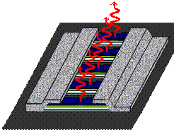
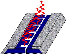
THz radiation, whose frequency range lies between microwaves and infrared light in the electromagnetic spectrum opens the possibility for a new imaging and spectroscopic technology with a broad range of applications, from medical diagnostic (without the damage produced by ionizing radiation such as X-rays) to industrial quality control or security-screening tools. THz signals must be obtained at the limits of electronics from one side and optical systems from the other, resulting in a lack of efficient and practical radiation sources. On the other hand, electronic devices able to detect or process signals at such high frequencies are quite scarce. The aim of this project is to develop advanced diodes and transistors able to generate, detect and process signals in the millimeter and submillimeter frequency ranges at room temperature. As sources of signals, we propose to exploit sub-THz and THz Gunn oscillations in novel (narrow- and wide-bandgap) semiconductor nanodevices: self-switching diodes (SSDs, both of InGaAs and GaN), and InGaAs slot diodes. As detectors, apart from standard THz Schottky diodes, resonant electron collective phenomena (like plasma oscillations) will be exploited in both diodes (InGaAs, InAs and InSb SSDs) and transistors (InGaAs HEMTs) to achieve enhanced sensitivity in specific THz frequency ranges. Finally, narrow-bandgap (InAs and InSb) HEMTs and ballistic nanodevices, with extremely high cutoff frequencies, will be optimized to process low-power signals near the
THz range; wide-bandgap (GaN) HEMTs being used for high power applications in the millimeter range. Monte Carlo simulations will be employed to analyze the physical processes underlying the operation of the devices and to design optimized structures. Devices will be fabricated in several laboratories that collaborate with the group executing the project. Feedback between fabrication technology and simulations will be promoted along the development of the project. Characterization of fabricated devices in the THz range will be performed also by collaborating laboratories. In the case of RF measurements, it is planned to complete the setup of a characterization laboratory in Salamanca with the acquisition of high-frequency equipment, so that part of the measurements to be performed in HEMTs and ballistic nanodevices will be directly carried out by the research team in charge of the project.